Unveiling the Nanoscale World: Raman Imaging of Graphene
Graphene, the wonder material of the 21st century, continues to captivate researchers with its extraordinary properties and potential applications. Its single-layer atomic structure, composed of carbon atoms arranged in a hexagonal lattice, gives rise to unparalleled mechanical strength, electrical conductivity, and thermal stability.
Raman spectroscopy, a non-destructive technique, provides invaluable insights into the structural, electronic, and vibrational properties of materials. When applied to graphene, it unveils a wealth of information about its quality, doping level, defects, and even its local environment.
Now couple the spectrometer to a microscope and we can spatially resolve this information. Imagine a graphene sample on a substrate. Traditional Raman spectroscopy would provide an average spectrum representing the entire sample. However, with Raman imaging, researchers can scan the sample systematically, collecting Raman spectra at each point. This spatially resolved data can then be used to create detailed images, also referred to as maps, of various graphene properties across the sample surface.
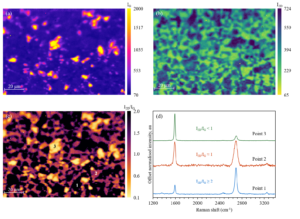
For instance, in pristine graphene, the Raman spectrum typically shows two prominent peaks: the G band (associated with in-plane vibrations of carbon atoms) and the 2D band (related to the second-order scattering process). By analysing the intensity, position, and width of these peaks across a graphene sample, researchers can assess its quality and layer thickness, Figure 1.

Figure 1. I2D/IG Raman mapping of graphene for layer number determination.
Moreover, Raman imaging can indicate areas of strain and defects. In materials science, it aids in quality control during graphene production processes, ensuring uniformity and desired properties. In the fabrication of devices, Raman imaging helps characterise graphene-components to optimise their performance. Read the full Application Note to learn more about Raman imaging of graphene.


